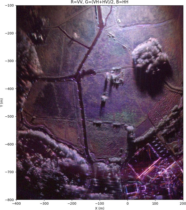
Uncalibrated SAR image
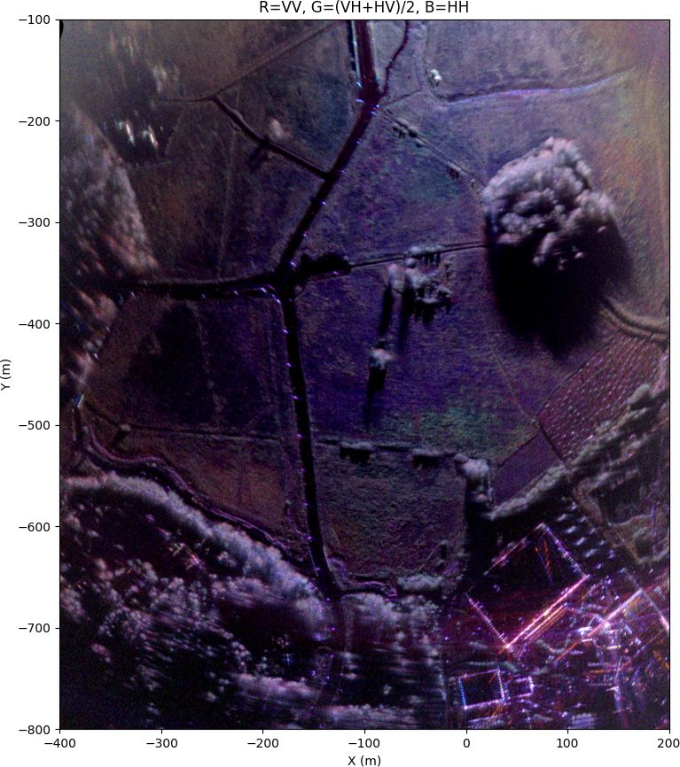
Same image after antenna pattern normalization and polarimetric calibration.
Wrote code for SAR image antenna pattern normalization and polarimetric calibration (channel imbalance and crosstalk). Image looks very nice now.
13.07.2025 14:10 — 👍 24 🔁 3 💬 2 📌 0
It's 10 seconds of data (10,000 radar pulses) and it takes about a minute to process.
12.06.2025 02:27 — 👍 2 🔁 0 💬 0 📌 0

Polarimetric synthetic aperture radar image
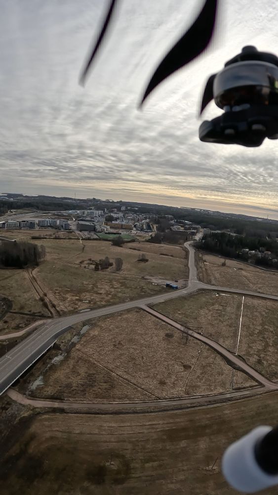
Camera photo of the same area.
I implemented a new SAR autofocus algorithm and now the image generation is both better and faster. It's about as well focused as it can be now.
11.06.2025 18:22 — 👍 12 🔁 0 💬 2 📌 0
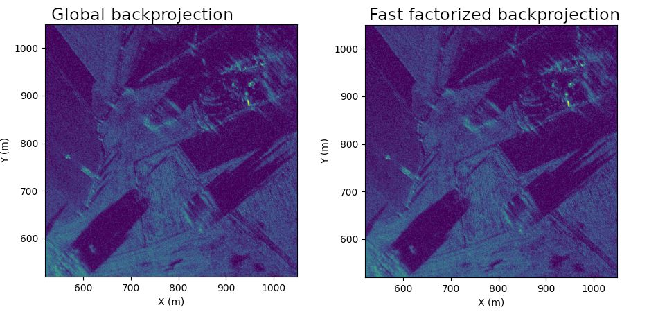
Fixed some bugs in my SAR processing code and now fast factorized backprojection generates a visually identical picture to the normal backprojection, but over 10 times faster. That's huge because normal backprojection was already extremely quick and there's still room for optimization with FFBP.
05.06.2025 17:34 — 👍 15 🔁 0 💬 0 📌 0
I also implemented generalized phase gradient autofocus earlier this week. I haven't seen any open source implementations of it before. It works quite well with this kind of short range SAR image, but my earlier minimum entropy optimization method still gives better results.
01.06.2025 17:42 — 👍 7 🔁 0 💬 0 📌 0

Global backprojection vs fast factorized backprojection image quality. The biggest difference is larger sidelobes on the brightest target in the FFBP image.
Found motivation to write some SAR processing code. Fast factorized backprojection generates several small polar format images and then interpolates them to one big image. It's faster, but has slightly worse image quality due to all the interpolations.
01.06.2025 17:42 — 👍 19 🔁 2 💬 1 📌 0
Just some random ones I had lying around. The bigger one is labeled: "XRRH6*10*3"
30.05.2025 08:03 — 👍 1 🔁 0 💬 0 📌 0
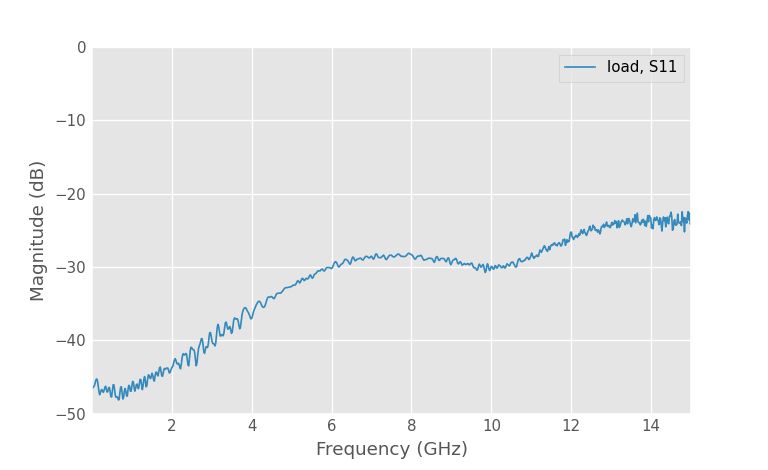
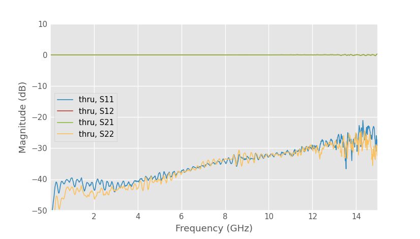
That's the measured S21 from input to the isolated port when the other ports are terminated. Reflection of the termination is not de-embedded, but it's better than -25 dB over the whole frequency range.
29.05.2025 12:57 — 👍 2 🔁 0 💬 0 📌 0
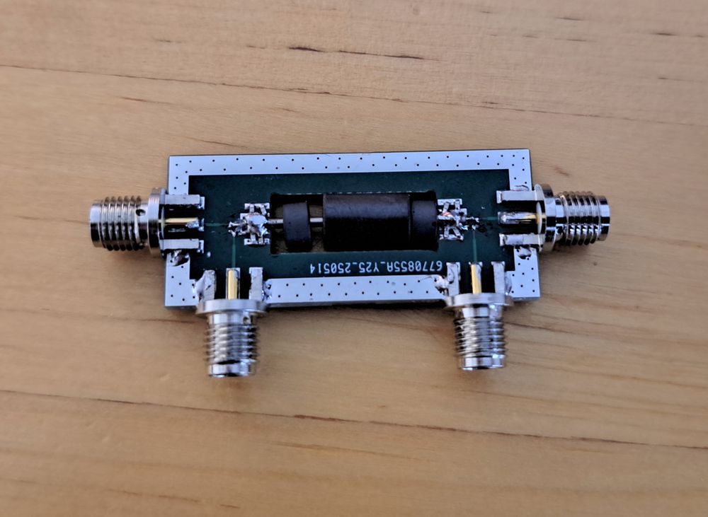
Dual directional bridge coupler PCB.
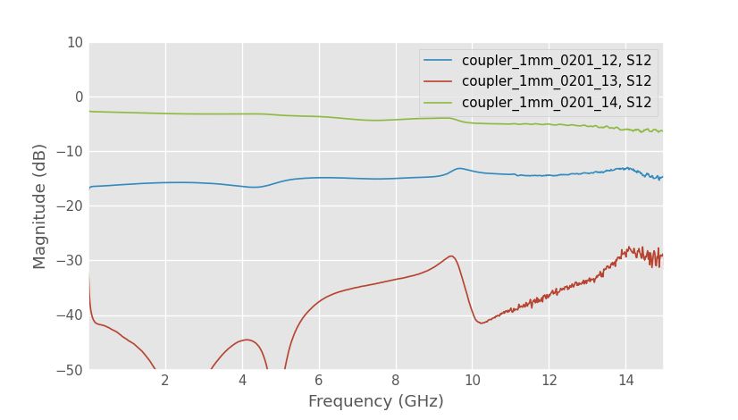
Thru, coupled, and isolated port S21 with other ports terminated.
I made this new dual directional bridge coupler using 1 mm diameter coaxial cable. It's a little bit better than the previous one I made using 2 mm coaxial cable and much more annoying to solder.
29.05.2025 07:41 — 👍 10 🔁 0 💬 2 📌 0
It works really well. Loss is low and matching is excellent.
28.05.2025 13:52 — 👍 5 🔁 0 💬 0 📌 0
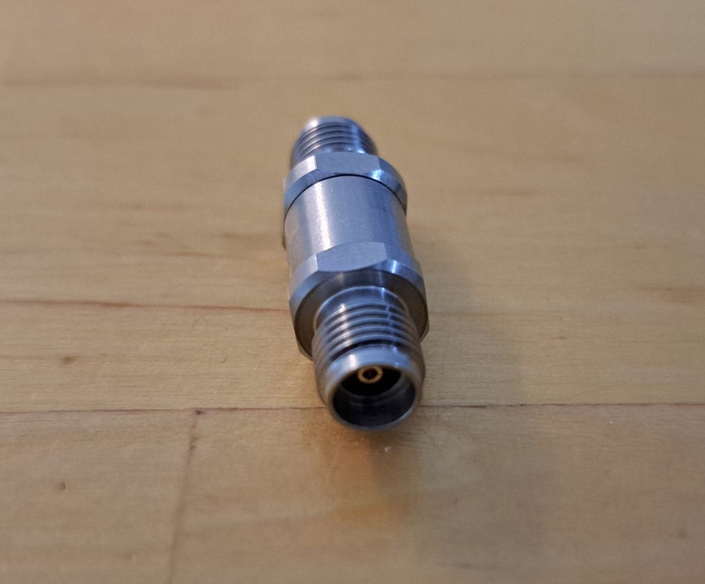
Bought this thru with 3.5mm RF connectors. It's air filled with just a thin see-thru membrane holding the center pin in place.
28.05.2025 13:52 — 👍 4 🔁 0 💬 2 📌 0

Two test PCBs with 3.5 mm and SMA connectors
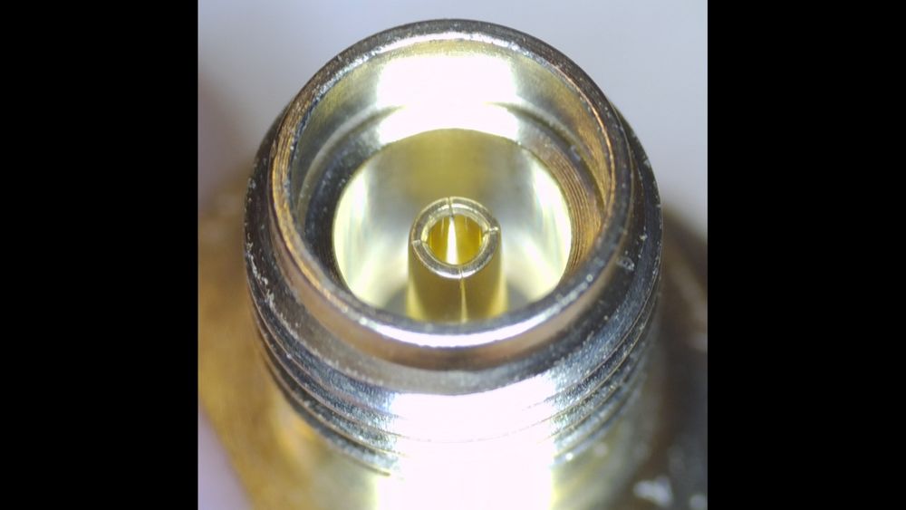
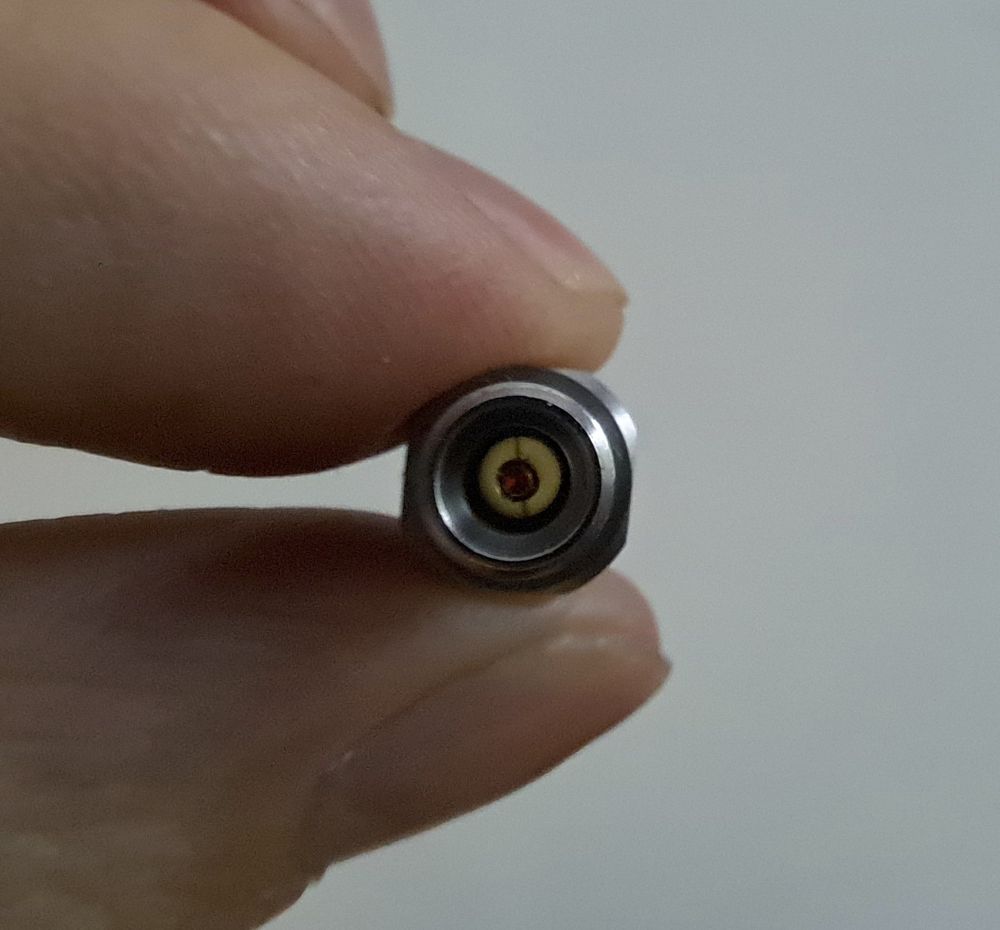
3.5 mm connector close up

3.5 mm and SMA connector S-parameters with 11 mm line
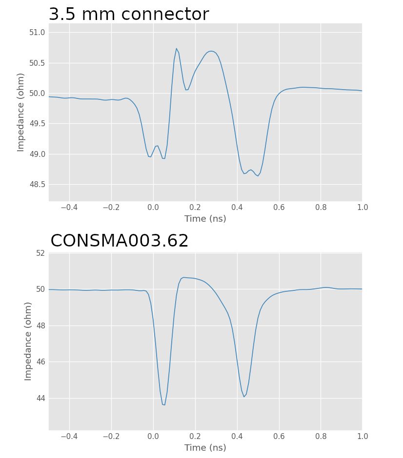
3.5 mm and SMA connector time domain response with 11 mm long line
Some new RF connector test PCBs. Nameless low-cost solderless 3.5 mm connector on the left and CONSMA003.062 clone on the right. Both work okay.
21.05.2025 14:37 — 👍 7 🔁 0 💬 1 📌 0
It would require hole and threads in the case for the connector making the case more expensive. Connector would also need to be soldered to the PCB while attached to the case, not very handy for a prototype.
15.05.2025 16:31 — 👍 0 🔁 0 💬 0 📌 0
It's this one: www.aliexpress.com/item/1005006.... Calibration coefficients are not included.
06.05.2025 15:44 — 👍 1 🔁 0 💬 1 📌 0
It's a very nice looking chip, but too expensive. Sure if someone else pays.
15.04.2025 20:32 — 👍 1 🔁 0 💬 0 📌 0
Just found an annoying flaw with this cheap bias-T. The connector is threaded in the case and if the cable is tightened with a torque wrench, it can unscrew also the SMA connector when removing the cable.
10.04.2025 16:39 — 👍 4 🔁 1 💬 1 📌 0
That could work in some situations, but I don't think it will work here. The connection between SMA connector and the case is not tightened so it wouldn't be compressed. Mating surface also isn't a full circle, just the upper part of the connector.
05.04.2025 18:57 — 👍 1 🔁 0 💬 1 📌 0
I thought this might be an issue during design. The proper fix would be to use a bulkhead SMA connector but that complicates the mechanical design and I didn't think it was worth the trouble.
05.04.2025 18:25 — 👍 4 🔁 0 💬 2 📌 0
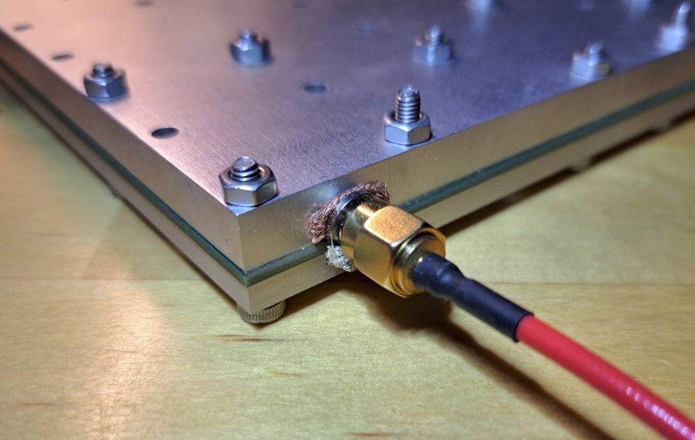
There's a tiny gap between the case and SMA connector that radiates a little if not sealed. Putting some solder wick in the gap seals it nicely but there has to be some more elegant method.
05.04.2025 18:25 — 👍 11 🔁 0 💬 2 📌 0
No, never thought there was enough interest to bother with that. This is fully self funded.
04.04.2025 14:33 — 👍 1 🔁 0 💬 1 📌 0
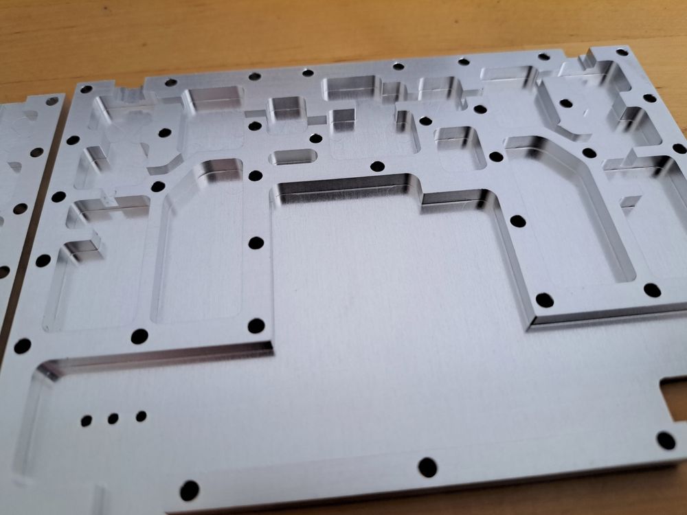
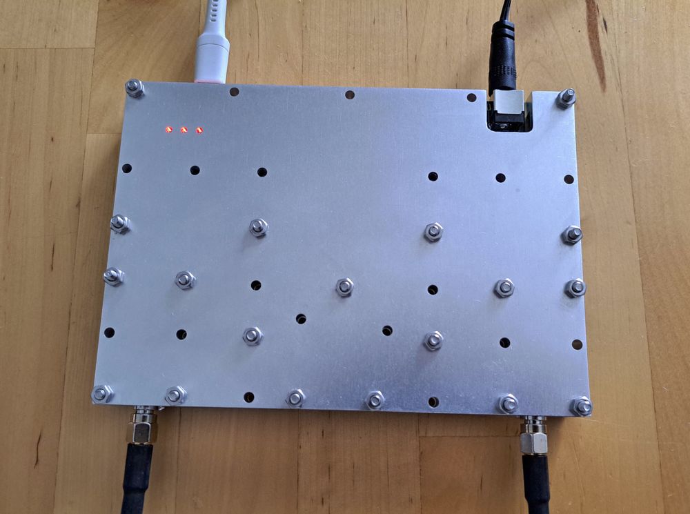
CNC machined case for the VNA just arrived. Machining quality is good and it looks stylish (very important). The cost was $140 including shipping and taxes, much cheaper than I initially feared.
04.04.2025 12:53 — 👍 50 🔁 4 💬 1 📌 0
Mechanical and temperature stability are currently the factors limiting the measurement accuracy. Electronics should be way more accurate than what I can currently measure.
24.03.2025 19:43 — 👍 3 🔁 0 💬 0 📌 0
VNA also works as a temperature sensor and strain gauge.
24.03.2025 19:40 — 👍 10 🔁 0 💬 1 📌 0
I doubt it's much better. This part really should be CNC machined from aluminium so that it would also function as heatsink.
24.03.2025 19:31 — 👍 0 🔁 0 💬 1 📌 0
It does get quite hot. FPGA internal temperature sensor says it's 70 degrees Celsius. I think the RF parts might run even hotter. 3D printed enclosure is a really poor heatsink.
24.03.2025 19:05 — 👍 2 🔁 0 💬 1 📌 0
This turned out to be slightly more difficult than I first thought. Foil tears easily and even a small tear will affect the isolation. It might require multiple layers to get a tear free lining. Foil also needs to be glued down so that it doesn't move around or it will increase drift of the VNA.
24.03.2025 18:53 — 👍 8 🔁 0 💬 4 📌 0
All drills were supposed to be 0.3 mm. Most pad diameters are 0.45 mm, but some are 0.40 mm. This used to be fine previously for no extra cost. I found few unintentional 0.2 mm drills with 0.5 mm pads and apparently this caused the extra charge?
23.03.2025 13:17 — 👍 0 🔁 0 💬 1 📌 0
Bellingcat | Ex-BBC R&D & Panorama | PhD in Electrical Engineering | He/Him
🌐 https://galen.reich.me.uk
big fan of computers and human beings.
🌍 Spatial Data Scientist | Team Lead | 🌱 AgTech | PhD in Computational Ecology + MSc in GIS
#rstats developer | geospatial engineering | soil microbiome and crop health mapping | product development
https://github.com/BlasBenito - www.blasbenito.com
🔥 Engineering knowledge exchange: http://hackaday.com
☠️ Get featured: tips at hackaday dot com
📒 Learn: http://hackaday.io/u
🇨🇦🇺🇦Grandfather, OSINT of Ukrainian and Russian Telegram: FPVs, drone munitions, EW, landmines. ❤️my family (grandchildren!), reading, and Kaja Kallas.
Colin is a huge nerd. Hardware hacking, open-source hardware, electronics design, academic stuff, dog stuff in some order. Assistant Prof @ Dalhousie Uni, advisor/co-founder NewAE Technology Inc.
Retired. IT background.
Radio Amateur, active mainly 28MHz - 10GHz.
Mostly digital modes, 10GHz EME
Enjoy working on radio related projects.
https://radio.g4hsk.co.uk/
Electronics & systems engineer, programmer, nerd.
Also spirit532@mastodon.social and @spirit532_ at the dumpster fire one.
Other socials and contact at https://spirit.re/
•Hobbyist and electronics enthusiast.
•Macro/Micro Photography.
•Microchip Decapping.
making open hardware at Opulo
deogie comics @deogie.bsky.social
pervis comics @pervis.bsky.social
software @kicad.org, hardware @formlabs
Sadly not a sci-fi author
Also at @craftyjon@chaos.social
he/him
Certified Electrical Engineering geek
I do electrical engineering videos and more at Keysight, podcasting and more at All About Circuits/EETech
Occasionally tweets will also include:
3D Printing
Mountain Biking
Youtube-ing
Marketing (ugh, I know)
PhD in Robotics, (embedded) Rust nerd, and embedded enthusiast. Develops and maintain http://rtic.rs.
Theoretical Physicist.
(She/her/hers)
From Eastern KY.
Illuminating math and science. Supported by the Simons Foundation. 2022 Pulitzer Prize in Explanatory Reporting. www.quantamagazine.org
Intern @ http://youtube.com/bpsspace