You know what time it is — see what this week’s word, gate-all-around (GAA) FET, is all about and why it matters: bit.ly/4ovKY4F
13.08.2025 16:54 — 👍 0 🔁 0 💬 0 📌 0
As global interest in AI increases, demands for expanded memory skyrocket — enter high bandwidth memory (HBM). Learn why advanced packaging technology is crucial to manufacturing HBM’s unique features. bit.ly/3JwZ0CM
12.08.2025 18:57 — 👍 0 🔁 0 💬 0 📌 0
Atomic layer etching (ALE), made possible with our Flex® products, removes ultra-thin, atomic layers of material — a crucial capability as devices continue to shrink in size. Learn more. www.lamresearch.com/technology/a...
06.08.2025 17:11 — 👍 1 🔁 0 💬 0 📌 0
Our ALTUS® Halo system delivers highly controlled molybdenum deposition, giving chipmakers a reliable path to meet the scaling and performance demands of future devices.
Tune into the video for more.
05.08.2025 17:35 — 👍 1 🔁 0 💬 0 📌 0
Think patterning can’t get cleaner? 💡 Our plasma etch keeps defects so low, it’s like searching every block of Shanghai for trash and spotting just one watermelon seed.
Take a closer look at the etch tools we offer like Akara® and Kiyo® — built to set the standard for precision. bit.ly/4mji5qd
04.08.2025 17:33 — 👍 1 🔁 0 💬 0 📌 0
Seed layer — our Word of the Week — is a microscopic foundation that helps deposition layers form with precision and purpose.
30.07.2025 17:58 — 👍 1 🔁 0 💬 0 📌 0
Building on 20+ years of industry-leading conductor etch products, Akara® raises the bar.
Dive into our newest conductor etch tool for the Sense.i® platform. ⬇️
29.07.2025 19:01 — 👍 1 🔁 0 💬 0 📌 0
Layers make the chip. Deposition makes the layers. From tiny pathways to protective barriers, every film is essential in chipmaking — and precision is everything. Read more about it via our Semi 101 blog. bit.ly/4078QSi
22.07.2025 17:50 — 👍 2 🔁 0 💬 0 📌 0
We’re back with another Word of the Week! This time, it’s inflection. Every now and then, chipmaking reaches an inflection point — a change in process technology so significant that it opens the door to new manufacturing capabilities.
16.07.2025 17:31 — 👍 4 🔁 0 💬 0 📌 0
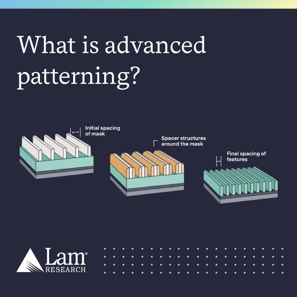
Next-generation semiconductor devices require advanced chips with the smallest features ever produced. Discover how our advanced patterning solutions enable these ultra-small features for logic, DRAM, and NAND devices. bit.ly/3GJTmMO
15.07.2025 23:12 — 👍 4 🔁 0 💬 0 📌 0
Happy Word of the Week Wednesday! This week’s word is high aspect ratio (HAR), which describes tall and narrow chip structures. Learn how our cryogenic technology enables vertical HAR profiles. bit.ly/46vlFHp
09.07.2025 18:40 — 👍 2 🔁 0 💬 0 📌 0
Inside every chip is a maze of tiny highways moving signals at high speed. As AI demands more, those highways need an upgrade. Enter molybdenum: better flow & fewer layers than tungsten. Explore what this means for chipmakers via our Semi 101 blog. bit.ly/4izxyR3
08.07.2025 17:39 — 👍 2 🔁 0 💬 0 📌 0
No one knows wafer fabrication equipment like we do. In fact, nearly all end-market devices — from satellites to smartphones — can be traced back to our tools or services. See how we help our memory, foundry, and logic customers make today’s technology possible. bit.ly/3ST44Dr
01.07.2025 16:24 — 👍 1 🔁 0 💬 0 📌 0
From secret projects in our garage lab to developing the world’s first copper plating product, SABRE®, our journey in Tualatin, Oregon, transforms chip production across the U.S. and beyond. See how it all started. ⬇️https://bit.ly/3ZVKqKL
30.06.2025 22:16 — 👍 2 🔁 0 💬 1 📌 1
At Lam, we make deposition effortless.
Learn how our thin film deposition products provide the precision, performance, and flexibility needed for a wide range of device applications. www.lamresearch.com/products/our...
26.06.2025 17:46 — 👍 1 🔁 0 💬 0 📌 0
Chip development is complex and expensive. By simulating tools and processes before anything physical is built, digital twins enable smarter ways to test ideas, solve problems, and cut costs in real time. Learn more via the blog. bit.ly/3YqU869
24.06.2025 19:12 — 👍 1 🔁 0 💬 0 📌 0

What happens when you mix science, creativity, and a million-dollar microscope? 🔬
You get Lam’s Microscopy Technician Training Program — a hands-on course with Portland Community College that just graduated its first class.
The future of semiconductor manufacturing starts here. 💡 bit.ly/4lfrH4L
20.06.2025 16:33 — 👍 1 🔁 0 💬 0 📌 0
What powers the storage capacity of your devices? Our Word of the Week holds the answer: 3D NAND.
This device architecture arranges memory cells vertically, rather than horizontally, to dramatically increase memory bit density. 💡
18.06.2025 17:38 — 👍 1 🔁 0 💬 0 📌 0
Want to learn more about the semiconductor industry? We got you covered.
Dive into our Semi 101 series for educational learnings — from digital twins to memory devices and more. bit.ly/4kDwUDA
17.06.2025 18:29 — 👍 0 🔁 0 💬 0 📌 0
Introducing Word of the Week — a series to help you brush up on Lam-related terms! This week’s word: DRAM. 💡
Ever wonder how your computer juggles so many tasks at once? DRAM acts as your device’s short-term memory, constantly refreshing stored data to keep things running smoothly.
11.06.2025 17:55 — 👍 0 🔁 0 💬 0 📌 0
Scaling 3D NAND past 200 layers requires precise control over etching, stress management, and material deposition. How do engineers pull it off? Watch the video to find out. bit.ly/3HvnZFG
10.06.2025 18:02 — 👍 0 🔁 0 💬 0 📌 0
At Lam Research, we pursue innovations that push beyond the boundaries of technical limitations, providing solutions that empower chipmakers to create the next generation of semiconductor breakthroughs.
Explore how we achieve the unthinkable. bit.ly/4l3byQ5
09.06.2025 19:08 — 👍 1 🔁 0 💬 0 📌 0