Quien es Monse? Otra IA? 😂🤣
03.01.2026 11:22 — 👍 0 🔁 0 💬 1 📌 0
El mundo ha perdido un gran alfarero!
03.01.2026 11:15 — 👍 2 🔁 0 💬 0 📌 0

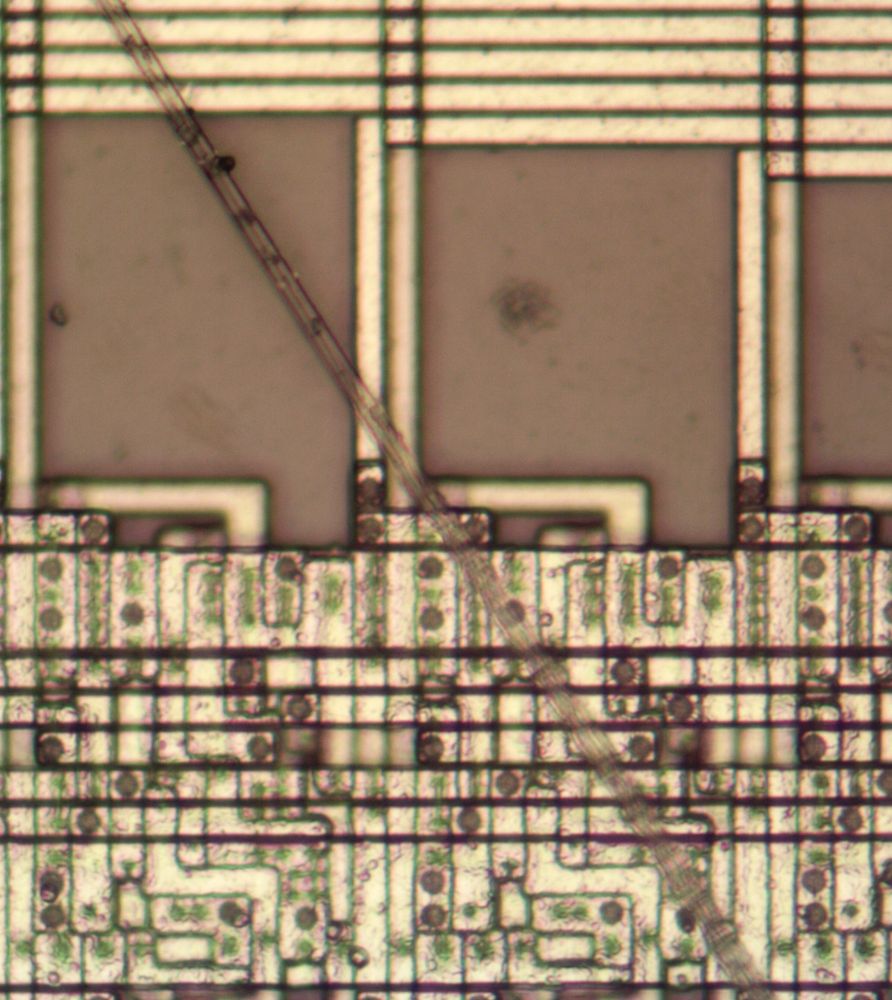
A photo of the 8087 die under a microscope. The die is rectangular, with complex patterns in purplish-brown. The patterns consist of rectangular regions, striped regions in the bottom half of the chip, and other more irregular regions.
At the right, two regions are highlighted in red: the registers and the stack control circuitry.
Around the edges of the die, you can see the hair-thin bond wires that connect the chip to its 40 external pins. The complex patterns on the die are formed by its metal wiring, as well as the polysilicon and silicon underneath. The bottom half of the chip is the "datapath", the circuitry that performs calculations on 80-bit floating point values. At the left of the datapath, a constant ROM holds important constants such as π. At the right are the eight registers that form the stack, along with the stack control circuitry. The chip's instructions are defined by the large rectangular microcode ROM in the middle.
In 1980, Intel announced the 8087 Math Coprocessor, a chip that made floating-point 100 times faster. I opened up the chip, took photos of the silicon structures, and analyzed its circuitry. It's a very complex chip for its time. Let's take a look inside...
09.12.2025 18:38 — 👍 127 🔁 34 💬 4 📌 1

A die photo of the 386 processor. It is a square with complicated patterns on top. Under the microscope, the circuits appear in dark purple. Parts of the chip have been marked with boxes: these are standard cell circuits and have a distinctive striped appearance.
Intel's 386 processor (1985) was critical to the success of Intel. With 285,000 transistors, it was too much for Intel's design process and the schedule started slipping. Intel pivoted to "standard cells", an automated technique for chip layout to get back on track. Let's look closer...
22.11.2025 16:56 — 👍 99 🔁 15 💬 3 📌 0

Quién es Jesucristo, el profeta al que homenajea Rosalía con su nuevo look: pasó una mala noche después de una cena con amigos
30.10.2025 22:01 — 👍 1514 🔁 415 💬 72 📌 59

Baterías: "Cuanto más baja el precio, más se acelera su adopción, y cuanto más se acelera su adopción, más baja el precio."
Y en diciembre empieza la producción en masa de baterías de sodio, cuyo coste puede llegar a ser un 90% menor que las de litio actuales.
Es hora de electrificarlo todo.
04.11.2025 09:52 — 👍 350 🔁 179 💬 7 📌 6
BambooHR
Seguimos creciendo en el equipo buscando personas que nos ayuden en nuestra misión de reducir el impacto de incendios forestales y eventos de clima extremo.
Buscamos un desarrollador BE con experiencia en .Net.
Si tienes cualquier duda, escríbeme.
technosylva.bamboohr.com/careers/149
05.11.2025 07:47 — 👍 2 🔁 2 💬 0 📌 0

Heat map-style graphic showing monthly air temperature rankings in the Arctic at the 925 hPa level for each month from January 1979 to October 2025. There is a long-term warming trend evident in each month. Blue shading is shown for colder months, and red shading is shown for warmer months. A yellow number is shown for each grid box to display the actual temperature ranking. October 2025 was the 4th warmest October on record.
Not every month will set a new record, but the warming trend is obvious. This graphic shows #Arctic air temperature rank by month over the satellite era - now updated through October 2025... 🧪
+ Ranks: 1=warmest (red), 46/47=coldest (blue)
+ Download higher resolution: zacklabe.com/arctic-tempe...
06.11.2025 20:59 — 👍 139 🔁 61 💬 1 📌 3
Hay enfermedades que sí que se curan con Fe. Como la anemia.
27.09.2025 13:36 — 👍 339 🔁 84 💬 15 📌 3
 26.09.2025 08:01 — 👍 23 🔁 9 💬 2 📌 1
Acabamos de sacar una posición que es una oportunidad que no se da mucho. Buscamos a un Technical Lead Manager, es decir a un manager que lidere un pequeño equipo y también ponga liderazgo técnico. Lo especial es que no importa que tenga poca experiencia gestionando porque tanto @javierdearcos.com
19.09.2025 07:25 — 👍 6 🔁 12 💬 1 📌 0
Era broma. No he visto ninguno técnico por ahí... deben estar en el despacho :)
PD: me mola tu clasificación por colores 😄
19.09.2025 08:44 — 👍 2 🔁 0 💬 1 📌 0
El libro de Java 1.2 creo que ya es hora de tirarlo 😁
18.09.2025 10:02 — 👍 1 🔁 0 💬 1 📌 0
YouTube video by Madrid JUG
Novedades Java 25
¡Ya está publicado el video con todas las novedades de #Java 25 que vimos ayer! 🚀
www.youtube.com/watch?v=6dA7...
17.09.2025 07:35 — 👍 14 🔁 7 💬 0 📌 0

🚀 ¡Estamos de vuelta tras el verano!
Y qué mejor que arrancar con la presentación de #Java 25 ☕️
Únete a nuestra charla grupal sobre todas las novedades
📅 Mar 16 Sep 19:00
📍 Oficinas de Celonis
🧑🏼🤝🧑🏼 www.meetup.com/madridjug/ev...
¡No te la pierdas! 👇🏼
04.09.2025 09:08 — 👍 8 🔁 8 💬 1 📌 2
All of the penicillin in use worldwide comes from a strain of mold that was growing on a cantaloupe bought at a grocery store in Peoria, Illinois in 1942.
10.08.2025 02:13 — 👍 3601 🔁 751 💬 45 📌 32

🎯💯
10.08.2025 03:10 — 👍 109 🔁 18 💬 1 📌 1
Me parece una exageración lo de 2 PMs por developer o que el PM desaparezca. Lo que si veo es que ell PM absorba ciertas cosas que hace el desarrollador y el desarrollador cosas que hace el PM. Difuminando la frontera de los roles
20.07.2025 09:05 — 👍 3 🔁 0 💬 1 📌 1
 16.07.2025 09:47 — 👍 577 🔁 175 💬 19 📌 7
El problema es llamarlo adaptación... digamos inspiración.
Usa las ideas principales de los libros y construye una historia nueva.
A mi, aceptando eso, me está gustando la serie
20.07.2025 08:53 — 👍 1 🔁 0 💬 0 📌 0
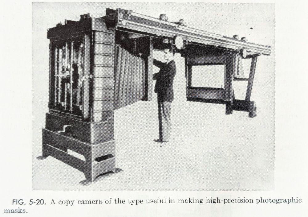
Black and white photo of a giant bellows camera about 8 feet tall. A man is standing in front of the lens which is the size of his torso. Caption: "A copy camera of the type useful in making high-precision photographic masks."
In the 1960s, this absurdly large camera was used to make masks for integrated circuits. The layers of the integrated circuit were drawn at large scale and then optically shrunk to make the glass masks that were used in manufacturing.
25.06.2025 17:33 — 👍 80 🔁 21 💬 4 📌 1
🧵 I’ve reviewed conference talk submissions for +10 years. Here are my tips:
(Side note, I've sinned against all these tips myself 🙃)
09.06.2025 11:48 — 👍 52 🔁 22 💬 2 📌 6

Un comodín del Balatro con la cara pixelada de Antonio Lobato. El nombre del comodín es "¿Cuánto vale tu coche?" y la descripción dice "cuando seleccionas tu coche, lo envía a la sucursal más cercana y gana el precio de tu coche al final de la ronda".
¿¿ANTONIO BALATRO??
25.05.2025 13:50 — 👍 803 🔁 504 💬 7 📌 10
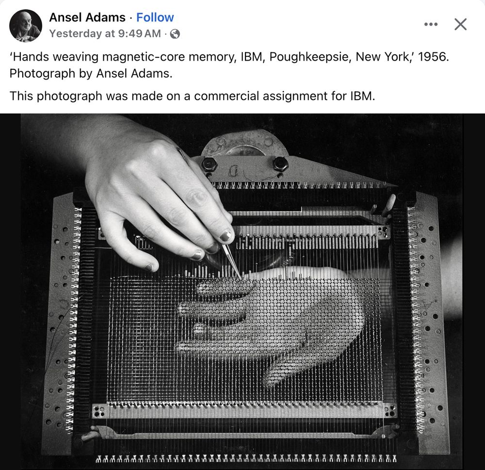
A photo with the caption "'Hands weaving magnetic-core memory, IBM, Poughkeepsie, New York', 1956. Photograph by Ansel Adams. This photograph was made on a commercial assignment for IBM."
This black-and-white photo shows a core memory plane being assembled. It consists of an 80 by 50 grid of wires in a frame with tiny toroids on the wire intersections. Each wire is attached to metal terminals on the frame. Someone is using tweezers to thread the tiny cores onto the wires. The plane is about 4/5 completed. One hand is below the plane, palm-up, visible through the wires. The other hand (with nail polish) is above the plane, holding tweezers.
This photo of magnetic core memory popped up, taken by Ansel Adams. I investigated a bit: this memory holds 4000 bits, each stored in a tiny magnetized ferrite ring. It may be from an IBM 705 vacuum-tube business computer. 1/N
30.05.2025 17:38 — 👍 278 🔁 82 💬 11 📌 5
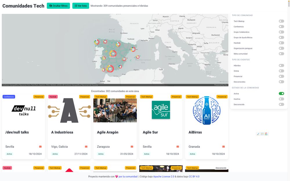
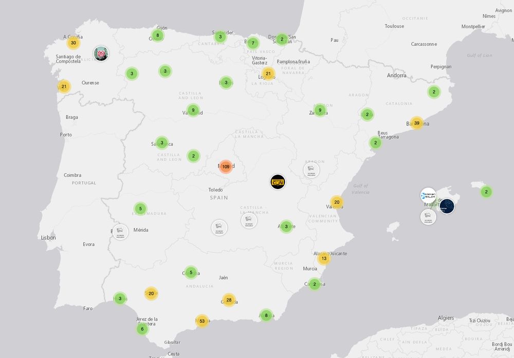
¿Sabes cómo están distribuidas estas +300 comunidades tecnológicas en España? Hoy hemos actualizado el repo añadiendo un mapa interactivo: github.com/ComBuildersE...
Como todo lo que hacemos, los datos son open data y el código bajo Apache v2, ¿nos ayudáis a difundirlo y mejorarlo?
19.05.2025 10:54 — 👍 17 🔁 12 💬 2 📌 2
A close-up of the die of the Intel 386 processor showing the metal layers. A strand of a spider web runs diagonally across the image. The processor image consists of yellowish metal wiring running horizontally and vertically, with more complex patterns underneath. Black circles indicate connections between the two metal layers. The spider web is about the same thickness as the metal wiring. The silicon circuitry underneath is not visible, but its feature size is 1.5 µm, considerably thinner than the spider web.
How thin is spider silk compared to the wiring on a chip? Here's a close-up of a spiderweb strand diagonally across an Intel 386 processor. The spiderweb is 4 µm thick, just a bit thinner than this 1985 chip's 5 µm metal wiring. Wiring in modern chips is 100 times thinner.
17.05.2025 19:01 — 👍 77 🔁 15 💬 2 📌 0
Your periodic reminder--if a design change is hard then you haven't worked hard enough making it easy.
01.05.2025 15:29 — 👍 64 🔁 24 💬 2 📌 0
Apache Arrow is the universal columnar format and multi-language toolbox for fast data interchange and in-memory analytics.
Find more at https://arrow.apache.org/
In love-hate relationship with machines. Currently: OpenJDK, AWS. "Trust me, it's really me" backlink: https://shipilev.net/#social
Customer Engineer at Google. Co-organizer @CommitConf.
Head of Developer Relations at Criteo R&D 🧡
Staff Engineer 🧑💻
#DevRel #TechCommunity
lecturer in recent runes, father of 2, husband, whistle player, videogames, geek, all things software engineering, java, cloud & devops at Accenture | MálagaJUG Lead | Java Champion
Asador del software, líder técnico y creador de contenido.
Impulsando a otros a desarrollar software con excelencia, impacto y principios.
Java Language Architect at Oracle. Author, Java Concurrency in Practice (http://amzn.to/2nzZnkl). Also, cats.
Tecnología, motos, música, desarrollo de software y algunos pensamientos #noArchitecture
⠠⠵
Para toda solución tengo un problema
Spanish software engineer, love scaling things. I consciously refuse to be driven by current events, or to have an opinion on everything, so I will probably never be an influencer.
Antropóloga agilista, experta en participación y amante del caos
Programmer building the future
Independent I guess these days you'd say content producer, artist, programmer, musician, pokerist. More about me at https://KentBeck.com.
Ingeniero hackeando para mejorar la Administración pública. Ayúdame a seguir en http://patreon.com/jaime_gomez_obregon
Computer history. Reverse-engineering old chips. Restored Apollo Guidance Computer, Alto. Ex-Google, Sun, Msft. So-called boffin.
https://www.juanignaciosl.com/